|
 小型光收發器之光學次模組裝置 小型光收發器之光學次模組裝置
|
刊登日期:2014/05/21 |
|
|
|
|
|
| ‧ 專利名稱 |
一種感測晶片之晶圓級封裝方法 |
| ‧ 專利證書號 |
I258210
US7,351,609B2
|
| ‧ 專利權人 |
國立臺灣大學 |
‧ 專利國家
(申請日) |
中華民國 (2005/04/18)
美國 (2006/03/22)
|
|
|
| |
| ‧ 發明人/PI |
吳恩柏,楊若群,
|
| ‧ 單位 |
應用力學研究所
|
| ‧ 簡歷/Experience |
|
|
| 技術摘要 / Our Technology: |
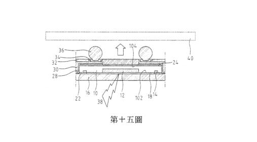
一種感測晶片之晶圓級封裝方法,其步驟包含:提供一包含有複數個晶元區域之晶圓,其晶元區域內包含一主動區及一位於該主動區周圍的銲墊;接合一透光保護層於該晶圓的第一表面上;形成一應力緩衝層於該晶圓的第二表面上;於兩晶元區域間的一預設位置上,藉由蝕刻或雷射鑽孔形成一通孔貫穿該應力緩衝層與該晶圓,以露出該銲墊或預設於兩該相鄰銲墊間之導線;以及形成複數個凸塊電極於該應力緩衝層上,藉由該通孔電性連接至該銲墊。本發明具有增進組裝便利性、降低製造裝配成本、及提高晶圓級封裝結構之可靠度等優點。
Method for wafer-level package of sensor chip includes following procedures: providing a wafer comprising multiple dies areas, which includes an active area and a weld pad located around the active area; surface mounting a transparent protection layer onto the first surface of the wafer; forming a stress bumper layer on the second surface of the wafer; forming a through hole penetrating the stress bumper layer and the wafer at a preset position between two dies areas via etching or laser drilling in order to expose the weld pad or a leading wire preset between two neighboring weld pads; forming multiple bump electrodes on the stress bumper layer to be electrically connected the weld pad by way of the through hole. The present invention has following advantages: assembling convenience, low assembly cost, high reliability of wafer-level package structure.
|
| 專利簡述 / Intellectual Properties: |
|
| |
聯繫方式 / Contact: |
| 臺大產學合作總中心 / Center of Industry-Academia Collaboration, NTU |
|
| Email:ordiac@ntu.edu.tw |
電話/Tel:02-3366-9945 |
|
|
| |
|
| |
 |


